In manufacturing of organic electronics, inkjet printing as an alternative technique for depositing materials is becoming increasingly important. Aside to the ink formulations challenges, improving the resolution of the printed patterns is a major goal. In this study we will discuss a newly developed technique to selectively modify the substrate surface energy using plasma treatment as a means to achieve this goal. First, we look at the effects of the μPlasma treatment on the surface energy for a selection of plastic films. Second, we investigated the effects of the μPlasma treatment on the wetting behaviour of inkjet printed droplets to determine the resolution of the μPlasma printing technique. We found that the surface energy for all tested films increased significantly reaching a maximum after 3-5 repetitions. Subsequently the surface energy decreased in the following 8-10 days after treatment, finally stabilizing at a surface energy roughly halfway between the surface energy of the untreated film and the maximum obtained surface energy. When μPlasma printing lines, an improved wetting abillity of inkjet printed materials on the plasma treated areas was found. The minimal achieved μPlasma printed line was found to be 1 mm wide. For future application it is important to increase the resolution of the plasma print process. This is crucial for combining plasma treatment with inkjet print technology as a means to obtain higher print resolutions.
DOCUMENT

In this article we investigate the change in wetting behavior of inkjet printed materials on either hydrophilic or hydrophobic plasma treated patterns, to determine the minimum obtainable track width using selective patterned μPlasma printing. For Hexamethyl-Disiloxane (HMDSO)/N2 plasma, a decrease in surface energy of approx. 44 mN/m was measured. This resulted in a change in contact angle for water from <10 up to 105 degrees, and from 32 up to 46 degrees for Diethyleneglycol-Dimethaclylate (DEGDMA). For both the nitrogen, air and HMDSO/N2 plasma single pixel wide track widths of approx. 320 μm were measured at a plasma print height of 50 μm. Combining hydrophilic pretreatment of the glass substrate, by UV/Ozone or air μPlasma printing, with hydrophobic HMDSO/N2 plasma, the smallest hydrophilic area found was in the order of 300 μm as well.
DOCUMENT
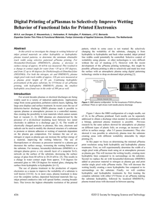
Inkjet printing is a rapidly growing technology for depositing functional materials in the production of organic electronics. Challenges lie among others in the printing of high resolution patterns with high aspect ratio of functional materials to obtain the needed functionality like e.g. conductivity. μPlasma printing is a technology which combines atmospheric plasma treatment with the versatility of digital on demand printing technology to selectively change the wetting behaviour of materials. In earlier research it was shown that with μPlasma printing it is possible to selectively improve the wetting behaviour of functional inks on polymer substrates using atmospheric air plasma. In this investigation we show it is possible to selectively change the substrate wetting behaviour using combinations of different plasmas and patterned printing. For air and nitrogen plasmas, increased wetting of printed materials could be achieved on both polycarbonate and glass substrates. A minimal track width of 320 μm for a 200 μm wide plasma needle was achieved. A combination of N2 with HMDSO plasma increases the contact angle for water up from <100 to 1050 and from 320 to 460 for DEGDMA making the substrate more hydrophobic. Furthermore using N2-plasma in combination with a N2/HMDSO plasma, hydrophobic tracks could be printed with similar minimal track width. Combining both N2 -plasma and N2/HMDSO plasma treatments show promising results to further decrease the track width to even smaller values.
DOCUMENT

Plasma treatment is a commonly used technology to modify the wetting behavior of polymer films in the production process for, e.g., printed electronics. As the effect of the plasma treatment decreases in time, the so-called "aging effect", it is important to gain knowledge on how this effect impacts the wetting behavior of commonly used polymers in order to be able to optimize production processing times. In this article the authors study the wetting behavior of polyethylene naphthalate (PEN), polyethylene terephthalate (PET), polycarbonate (PC), fluorinated ethylene propylene (FEP) and polyimide (PI) polymer films after plasma treatment in time. The plasma treatment was performed using a novel maskless DBD plasma patterning technology, i.e., Plasma Printing, at atmospheric pressure under nitrogen atmosphere. After treatment, the samples were stored at room temperature at 30%-40% relative humidity for up to one month. An increase in wettability is measured for all polymers directly after Plasma Printing. The major increase in wettability occurs after a small number of treatments, e.g., low energy density. More treatments show no further beneficial gain in wettability. The increase in wettability is mainly due to an increase in the polar part of the surface energy, which can probably be attributed to chemical modification of the surface of the investigated polymers. With the exception of FEP, during storage of the plasma treated polymers, the wettability partially declines in the first five days, after which it stabilizes to approximately 50% of its original state. The wettability of FEP shows little decline during storage. As the storage time between production steps is mostly under two days, Plasma Printing shows good promise as a pre-treatment step in the production of printed electronics. d c 2013 Society for Imaging Science and Technology.
LINK
With a market demand for low cost, easy to produce, flexible and portable applications in healthcare, energy, biomedical or electronics markets, large research programs are initiated to develop new technologies to provide this demand with new innovative ideas. One of these fast developing technologies is organic printed electronics. As the term printed electronics implies, functional materials are printed via, e.g. inkjet, flexo or gravure printing techniques, on to a substrate material. Applications are, among others, organic light emitting diodes (OLED), sensors and Lab-on-a-chip devices. For all these applications, in some way, the interaction of fluids with the substrate is of great importance. The most used substrate materials for these low-cost devices are (coated) paper or plastic. Plastic substrates have a relatively low surface energy which frequently leads to poor wetting and/or poor adhesion of the fluids on the substrates during printing and/ or post-processing. Plasma technology has had a long history in treating materials in order to improve wetting or promote adhesion. The µPlasma patterning tool described in this thesis combines a digital inkjet printing platform with an atmospheric dielectric barrier discharge plasma tool. Thus enabling selective and local plasma treatment, at atmospheric pressure, of substrates without the use of any masking materials. In this thesis, we show that dependent on the gas composition the substrate surface can either be functionalized, thus increasing its surface energy, or material can be deposited on the surface, lowering its surface energy. Through XPS and ATR-FTIR analysis of the treated (polymer) substrate surfaces, chemical modification of the surface structure was confirmed. The chemical modification and wetting properties of the treated substrates remained present for at least one month after storage. Localized changes in wettability through µPlasma patterning were obtained with a resolution of 300µm. Next to the control of wettability of an ink on a substrate in printed electronics is the interaction of ink droplets with themselves of importance. In printing applications, coalescence of droplets is standard practice as consecutive droplets are printed onto, or close to each other. Understanding the behaviour of these droplets upon coalescence is therefore important, especially when the ink droplets are of different composition and/or volume. For droplets of equal volume, it was found that dye transport across the coalescence bridge could be fully described by diffusion only. This is as expected, as due to the droplet symmetry on either side of the bridge, the convective flows towards the bridge are of equal size but opposite in direction. For droplets of unequal volume, the symmetry across the bridge is no longer present. Experimental analysis of these merging droplets show that in the early stages of coalescence a convective flow from the small to large droplet is present. Also, a smaller convective flow of shorter duration from the large into the small droplet was identified. The origin of this flow might be due to the presence of vortices along the interface of the bridge, due to the strong transverse flow to open the bridge. To conclude, three potential applications were showcased. In the first application we used µPlasma patterning to create hydrophilic patterns on hydrophobic dodecyl-trichlorosilane (DTS) covered glass. Capillaries for a Lab-on-a-chip device were successfully created by placing two µPlasma patterned glass slides on top of each other separated by scotch tape. In the second application we showcased the production of a RFID tag via inkjet printing. Functional RFID-tags on paper were created via inkjet printing of silver nanoparticle ink connected to an integrated circuit. The optimal operating frequency of the produced tags is in the range of 860-865 MHz, making them usable for the European market, although the small working range of 1 m needs further improvement. Lastly, we showed the production of a chemresistor based gas sensor. In house synthesised polyemeraldine salt (PANi) was coated by hand on top of inkjet printed silver electrodes. The sensor proved to be equally sensitive to ethanol and water vapour, reducing its selectivity in detecting changes in gas composition.
DOCUMENT

Using stable isotope techniques, this study shows that plasma free fatty acid oxidation is not impaired during exercise in non-obese type II diabetic patients.
DOCUMENT

Boven titel staat vermeld: De symbiose van biologie en technologie. Zowel vanuit het Applied Science onderwijs als vanuit het werkveld kwam er meer vraag om biologische expertise toe te voegen aan het bestaande lectoraat Thin Films & Functional Materials.
DOCUMENT

This letter to the editor argues that the assumption of a single value for the acetate recovery factor in carbon-13 stable isotope research for different individuals, can lead to significant errors in the outcomes of substrate utilization measurements.
DOCUMENT

The data of this study indicate that the acetate recovery factor, used in stable isotope research, needs to be deteremined in every subject, under similar conditions as used for the tracer-derived determination of substrate oxidation.
DOCUMENT

In deze publicatie wordt ingegaan op het verbinden van dunne plaat en buis met behulp van de diverse verbindingsprocessen. Deze publicatie is er een uit een serie van vijf die naast deze algemene publicatie tevens vier verbindingstechnieken behandelen, zoals lassen (TI.03.14), lijmen (TI.03.15), mechanisch verbinden (TI.03.16) en solderen (TI.03.17).
DOCUMENT

